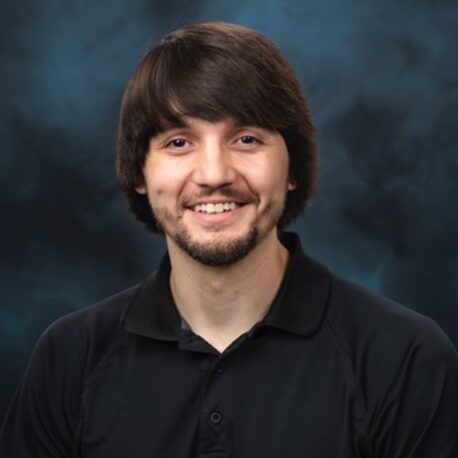
Speaker Bio

Michael J. Zachman
Oak Ridge National Laboratory, “Advanced Electron Microscopy for Energy Storage and Conversion Materials Research”
Abstract:
Development of enhanced energy storage and conversion devices is critical for accelerating our transition to a sustainable future. The performance, durability, and safety of these devices often depend highly on the nano- to atomic-scale properties of the materials and interfaces within them, making an understanding of their local properties critical for enabling progress. While a variety of characterization techniques are available that can provide a wealth of information, many lack the spatial resolution required to directly capture heterogeneities at these scales. High-resolution scanning transmission electron microscopy (STEM) and spectroscopy are therefore valuable tools for directly probing local structural and electronic properties of materials in real space. The high-energy electron beam, high-vacuum sample environment, image contrast mechanisms, and typical low fields of view (FOVs) of conventional techniques can limit the types of materials that can be characterized and the robustness of measurements performed, however. In this talk, I will describe advanced electron microscopy techniques designed to address these limitations by providing access to new materials and increasing the quantity and quality of information obtainable. First, I will show how cryogenic techniques enable the structure and chemistry of solid-liquid interfaces, such as electrode-electrolyte interfaces in Li-metal batteries, to be explored at the nanoscale with liquids and reactive materials intact. Next, I will discuss how “four-dimensional” STEM imaging techniques allow the structure of battery and fuel cell materials consisting of a range of elements to be visualized at the atomic scale in a directly interpretable manner. Finally, I will demonstrate how automation enables orders of magnitude more information to be acquired in a single experiment, allowing measurements to be performed across large FOVs, such as entire electrode cross sections, while maintaining high spatial resolution. Techniques such as these provide critical insights into the local properties of energy conversion and storage materials and devices, advancing progress toward next-generation devices important for enabling a sustainable future.
Speaker’s Bio:
Michael Zachman is a Staff Scientist in the Center for Nanophase Materials Sciences at Oak Ridge National Laboratory. He received his B.S. in Physics from Purdue University in 2012 and his Ph.D. in Applied Physics from Cornell University in 2018. Michael’s research interests lie in advancing electron microscopy techniques to provide an understanding of the structure and properties of energy and quantum materials down to the atomic scale. His doctoral work concentrated on developing cryogenic focused ion beam (cryo-FIB) and scanning transmission electron microscopy (cryo-STEM) techniques to study processes at solid-liquid interfaces at high resolution with liquids and reactive materials intact. Michael’s postdoctoral research focused on developing and applying four-dimensional STEM techniques to battery and two-dimensional materials to access to new aspects of their structure at nanometer and atomic scales. As a staff scientist, Michael has worked to advance hydrogen generation and conversion materials through techniques such as these in combination with automation strategies to increase the robustness and reliability of generated results.